Scanning Electron Microscopy/Energy Dispersive X-Ray Spectroscopy (Sem/Eds)
Scanning electron microscope (SEM) provides a high depth of field at large magnifications permitting a detailed study of the surface topography of materials. Examination of individual grains, dendrites, fracture surfaces, precipitate phases and corrosion products is routinely performed. Energy dispersive x-ray spectroscopy (EDS) coupled with SEM is used to determine chemical composition of micro-features.
Capabilities
- Imaging at high depths of field at large magnifications
- Imaging resolution of 3nm
- Secondary electron imaging, surface topography of materials
- Backscattered imaging of un-etched surfaces
- Low vacuum mode to examine non-conducting samples such as polymers
- Microchemical analysis of microstructural features such precipitates, phases, etc.
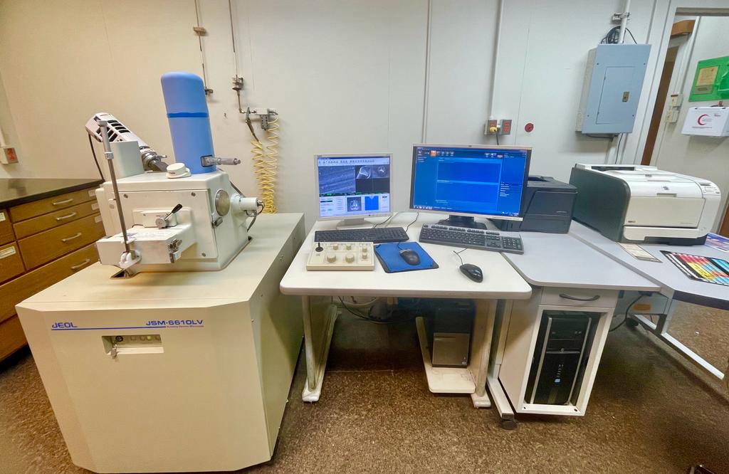
Facilities
- Model JEOL 5800LV- Tungsten filament, automated stage with X, Y, Z, tilt and rotational movement, airlock chamber, up to 30KeV accelerating voltage
- Materials identification, non-destructive chemical analysis, imaging of surface topography and microstructural features
- Computerized controls where data is obtained, stored and analyzed efficiently by a PC interfaced to the SEM
- Chemical analysis is performed using efficient EDS standard less method
- Charging effects are reduced by employing low vacuum mode
Location Scientist In-charge
Center for Engineering Research Name: Mr. AbdulKhaleq Bomwzah,
Phone: 860-4956 Phone: 860-1241