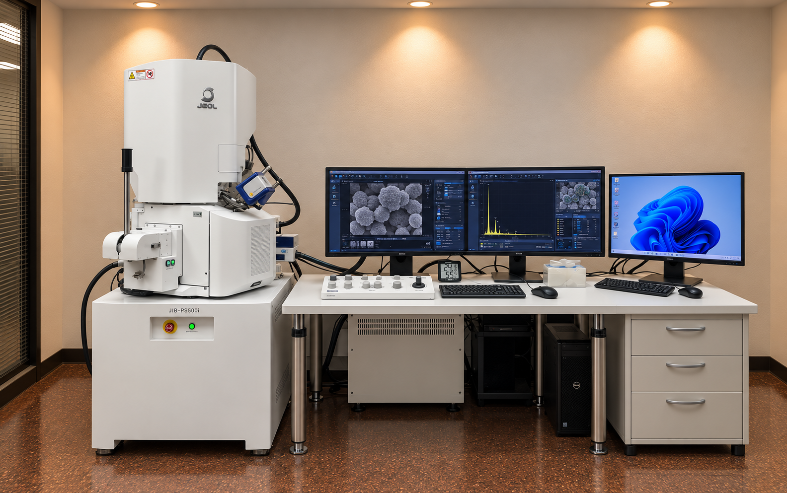
Focused Ion Beam–Scanning Electron Microscopy (FIB-SEM)
Focused Ion Beam–Scanning Electron Microscopy (FIB-SEM) is an advanced dual-beam technique used to investigate the microstructure, surface morphology, and internal features of materials. The JEOL JIB-PS500i combines a high-resolution field emission Scanning Electron Microscope (FE-SEM) with a focused gallium ion beam for precise material removal and imaging. The SEM provides detailed surface and cross-sectional images, while the FIB enables site-specific milling, sectioning, and preparation of electron-transparent specimens for TEM analysis. The system supports advanced sample preparation, structural characterization, and three-dimensional microstructural investigation through sequential milling and imaging. It is widely used in materials science, nanotechnology, semiconductor research, metallurgy, ceramics, battery materials, and failure analysis.
Capabilities
High-resolution Scanning Electron Microscopy (SEM) imaging
Focused Ion Beam (FIB) milling and precision material processing
Site-specific cross-sectional preparation and imaging
Ultrathin specimen preparation for TEM and STEM analysis
Nanoscale surface morphology and microstructural characterization
Three-dimensional microstructural analysis through serial sectioning
Grain boundary, interface, and defect investigation
Semiconductor device inspection and failure analysis
Elemental analysis and mapping using EDS when equipped
Applications: Semiconductors, metals, alloys, ceramics, nanomaterials, thin films, coatings, batteries, and advanced functional materials
Facilities
Model: JEOL JIB-PS500i
Manufacturer: JEOL Ltd.
Combined Focused Ion Beam and Field Emission Scanning Electron Microscope (FIB-FESEM)
Gallium (Ga) liquid metal ion source for precision milling
FIB accelerating voltage range: 0.5–30 kV
FIB beam current: 1 pA–100 nA
SEM landing voltage range: 0.01–30 kV
SEM imaging resolution: 0.7 nm at 15 kV
FIB imaging resolution: 3 nm at 30 kV
High-resolution Secondary Electron (SE) and Backscattered Electron (BSE) imaging
Computer-controlled five-axis motorized specimen stage
Automated beam control, imaging, and milling operations
Site-specific TEM specimen preparation and cross-sectional analysis
Integrated software for image acquisition and microstructural characterization
Location Equipment In-charge
Core Research Facilities Name: Mr. Syed Abrar Hussain
Building 61 LAB# 115 Phone: 860-3129
E-mail: syed.hussain@kfupm.edu.sa