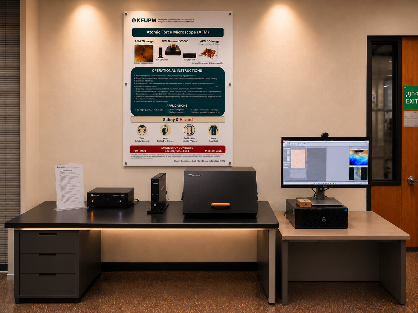
Atomic Force Microscopy (AFM)
Atomic Force Microscopy (AFM) is an advanced scanning probe microscopy technique used to characterize the surface structure and physical properties of materials at the nanometer scale. It operates by scanning a sharp probe across the sample surface and measuring the interaction forces between the probe and the material. The Nanosurf C3000 enables high-resolution two-dimensional and three-dimensional surface imaging, providing detailed information about surface roughness, particle dimensions, grain morphology, and surface features. This technique requires minimal sample preparation and can analyze both conductive and non-conductive materials. It is widely used in nanotechnology, materials science, semiconductor research, thin-film analysis, and coating characterization.
Capabilities
High-resolution two-dimensional and three-dimensional surface imaging
Nanometer-scale surface topography analysis
Quantitative surface roughness measurements (Ra, Rq)
Particle size and grain morphology analysis
Surface height and profile measurements
Thin-film and coating surface characterization
Analysis of conductive and non-conductive materials
Applications: Nanomaterials, polymers, ceramics, semiconductors, coatings, thin films, and composites
Facilities
Model: Nanosurf C3000
Manufacturer: Nanosurf
Scanning probe microscopy system for nanoscale surface characterization
High-resolution 2D and 3D surface topography imaging
Computer-controlled scanning and data acquisition
Integrated software for image processing and surface analysis
Quantitative surface roughness and height measurements
Surface morphology and particle dimension analysis
Nanoscale surface profile and texture characterization
Location Equipment In-charge
Core Research Facilities Name: Ms. Shahad Alzahrani
Building 15 LAB# 2215 Phone: 860-5819
E-mail: shahad.zahrani@kfupm.edu.com